The invention and subsequent development of scanning probe microscopy (SPM) methods have produced the necessary tools for a step
forward in optical measurements.
The possibility to go beyond the Abbe diffraction limit has been achieved with the Near-field light optical microscopes (SNOM). This is
employing the SPMs precision of piezoelectric raster-scanning together with small sharp optical probe to obtain optical images at subwavelength
resolution.
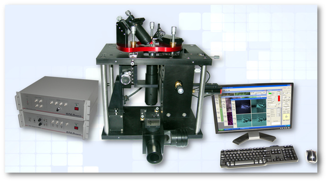
TriA-SNOM
TriA SNOM combines the potentials of scanned probe technology with the power of optical microscopy. It brings a small optical probe
very close to the sample surface, in the region called "near-field", and it allows the collection of optical signals providing image optical
resolution below 100 nm.
Key features:
-
Integrated Double Optical Vision System for accurate positioning and far field optical investigation
-
Compatible with a wide range of light microscope modes
-
Separate or simultaneous transmission and reflection measurements
-
Large Operation wavelength range
-
Allows the light source set-up as top down or inverted
-
Independent high-performance photo detectors for multiple optical signals collection.
-
Easily expandable
-
Compatibility with third party scientific equipments
Applications:
Imaging the optical properties of a sample with resolution below the diffraction limit with applications in nanotechnology,
biological studies, polymer investigations study of semiconductor materials
SNOM Working modes:
SNOM Topography: The image obtained is the result of signals acquisition in xyz axis that allows to measure detailed surface morphology and nanostructures on a nanometric scale.
SNOM Optical Reflection: image is obtained with near-field light that interacts locally with a superficial layer of the sample, giving information on structures confined within 30-100 nm (depending on the tip aperture) below sample surface.
SNOM Optical Transmission: the image results from the light transmitted through the whole thickness of the sample. While in conventional optical microscope all the sample is illuminated, SNOM near-field light interacts only locally producing signals point by point. SNOM optical transmission images are comparable with conventional optical images but their lateral resolution is more than 10 times higher.
SNOM Optical Back-Reflection: image is created by the near-field light that is back-reflected into the fiber, after local interaction with the sample surface.
TriA SNOM Scanning system
Scanning stage with absolute positioning system and strain gauge sensors.
Standard scanner technical data:
X-Y scan size:
-
100 x 100 μm (high voltage mode)
-
10 x 10 μm (low voltage mode)
-
High voltage closed loop resolution: 2 nm
-
High voltage open loop resolution: 0.2 nm
-
Closed loop linearity: 0.1%
Z scan size:
-
10 μm (high voltage mode)
-
1 μm (low voltage mode)
-
Resolution: 0.16 nm (high voltage mode), 0.02 nm (low voltage mode).
Based on specific demands other scanning ranges can be combined by the user in different configurations*.
Maximum sample size: it can accommodate samples with different geometries and sizes up to 30 mm diameter.
SPM Control System
It is composed by a digitally controlled analog feedback that combines the flexibility of computer controlled parameters with the high resolution and low noise of an analogue implementation. This detection scheme provides sub-nanometric vertical resolution in the images and all collected signals are distortions free.
The electronics supports STM, AFM and SNOM heads, performs different kinds of spectroscopy and can acquire several user-defined auxiliary channels.
Acquisition software
Software runs under Windows and is composed of a multi- window application to control the instrument and do the data acquisition. The software controls all the parameters of the instrument.
Tools & Accessories
TriA SNOM can be equipped with a large number of laser sources and filters

Our TriA SNOM integration with Princeton Instruments Monovista Acton Raman spectrograph.